
Free-Space Balanced Amplified Photodetectors
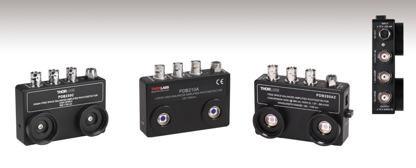
- Wavelengths Covering the 190 - 1700 nm Range
- DC to 1 MHz or DC to 100 MHz Bandwidths
- Detectors with Diameters Up to 5 mm
- Common Mode Rejection Ratio ≥30 dB
PDB230C
InGaAs Photodetector
for 800 - 1700 nm
PDB210A
Si Photodetector
for 320 - 1060 nm
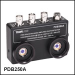
Top Panel of
the PDB250A
PDB250A2
Switchable Gain
UV-Enhanced Si Photodetector
for 190 - 1060 nm
OVERVIEW
| Balanced Detector Selection Guide |
|---|
| Balanced Detectors with Fast Monitor Output |
| Free-Space Balanced Amplified Detectors |
| Suitable for OCT |
| Compact Balanced Amplified Detectors |
| Compact Balanced Detectors |
| OCT Balanced Detectors with Fast Monitor Output |
| Auto-Balanced Detector with Avalanche Photodiodes |
| Polarization-Dependent Balanced Detector |
Typical Applications
- Spectroscopy
- Heterodyne Detection
- Optical Coherence Tomography
- Optical Delay Measurements
- THz Detection
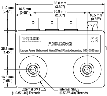
Click to Enlarge
Simplified Mechanical Drawing of the PDB220A2 Photodetector
Features
- Common Mode Rejection Ratio: ≥30 dB
- High Bandwidth: DC to 1 MHz or DC to 100 MHz
- Fixed and Switchable Gain Options
- Fixed Gain Item #'s: PDB220A2, PDB210x, PDB230x
- Switchable Gain Item #: PDB250x
- Ultra Low Noise (See the Specs tab for Model-Specific NEPs)
- Designed for Free Space Applications (Fiber Input Also Feasible)
- Direct Detector Monitor Outputs
- Includes Switchable Power Supply
- External SM1 (1.035"-40) Threads and Internal SM05 (0.535"-40) Threads
These Free-Space Balanced Amplified Photodetectors act as balanced receivers by subtracting the two optical input signals from each other, resulting in the cancellation of common mode noise. This allows small changes in the signal path to be extracted from the interfering noise floor. The PDB230x photodetectors have smaller active areas but wider bandwidth than the PDB220A2(/M), PDB210A(/M), PDB120C(/M), and PDB250x photodetectors (see the tables below).
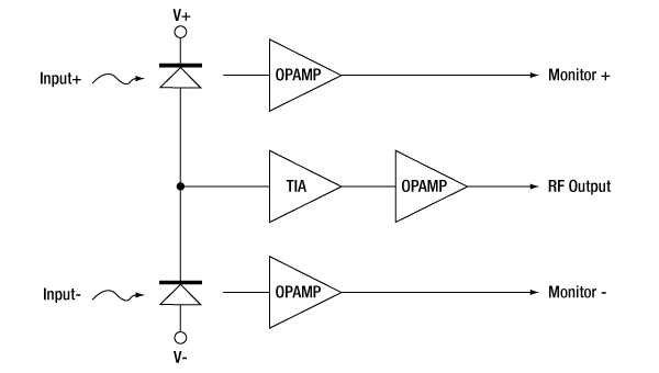
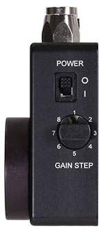
Each detector uses two well-matched Si or InGaAs detectors and an ultra-low-noise transimpedance amplifier for improved noise reduction. An output voltage (RF-OUTPUT) is generated that is proportional to the difference between the photocurrents in the two photodiodes (i.e., the two optical input signals). The PDB250x series of detectors feature a switchable gain setting with 8 steps and a range of 42 dB. Please see the Operation tab for more details. Additionally, the photodetectors have two fast monitor outputs (MONITOR + and MONITOR -) to measure optical input power levels as well as RF modulated signals on each detector.
The detectors are spaced 2" apart, making beam alignment an easy task on an optical table. To further simplify the use of these detectors, the housing has external SM1 (1.035"-40) and internal SM05 (0.535"-40) threads around each detector to attach components such as lens tubes, cage systems, mounted optics, and fiber collimator adapters. For compatibility with other externally SM1-threaded items, two SM1T1 adapters are included with each detector.
Electrical Connectors
Three BNC electrical connectors provide the balanced output signal plus a power monitor for each of the two input signals. These two monitors can be used as an independent power meter for each channel, which is helpful when adjusting the power level incident on each photodiode.
Housing/Power Supply
These balanced detectors are housed in a rugged, shielded aluminum enclosure. The housing allows a mounting post adapter to be fixed to the bottom or side surface by 8-32 (M4 x 0.7) screws. Each balanced detector is powered using an included LDS12B ±12 V DC power supply that has an input voltage of 100, 120, or 230 VAC that can be manually selected by a switch. Replacement LDS12B power supplies are available below.
Thorlabs also offers Fiber-Based Interferometers, which feature an integrated balanced detector.
SPECS
Fixed Gain Detectors
| Item #a | PDB220A2(/M) | PDB210A(/M) | PDB210C(/M) | PDB230A | PDB230C | |
|---|---|---|---|---|---|---|
| Detector Type | UV Enhanced Si/PIN | Si/PIN | InGaAs/PIN | Si/PIN | InGaAs/PIN | |
| Wavelength Range | 190 - 1100 nm | 320 - 1060 nm | 800 - 1700 nm | 320 - 1000 nm | 800 - 1700 nm | |
| Typical Maximum Responsivity @ Peak Wavelength |
0.5 A/W @ 960 nm | 0.6 A/W @ 920 nm | 1.0 A/W @ 1550 nm | 0.53 A/W @ 820 nm | 1.0 A/W @ 1550 nm | |
| Peak Wavelength | 960 nm | 920 nm | 1550 nm | 820 nm | 1550 nm | |
| Diameter of Active Detector Area | 4.1 mm | 5 mm | 3 mm | 0.8 mm | 0.3 mm | |
| Photodiode Damage Threshold | 20 mW | |||||
| Optical Input | Free-Space | |||||
| RF Output | ||||||
| Electrical Output | BNC, 100 Ω | BNC, 50 Ω | ||||
| Output Coupling | DC (AC-Coupling Available Upon Request) | |||||
| Bandwidth (3 dB) | DC - 1 MHz | DC - 100 MHz | ||||
| Common Mode Rejection Ratio (CMRR) Typical |
30 dB (Typical) | 40 dB (Typical) | 30 dB (Typical) | >30 dB 35 dB (Typical) |
>30 dB 40 dB (Typical) |
|
| Transimpedance Gain | High Z Load | 500 x 103 V/A | 50 x 103 V/A | |||
| 50 Ω Load | 175 x 103 V/A | 24.5 x 10³ V/A | ||||
| Conversion Gain @ Peak Wavelength |
High Z Load: 250 x 103 V/W | High Z Load: 300x103V/W | High Z Load: 500 x 103 V/W | 26.5 x 10³ V/W | 50 x 103 V/W | |
| 50 Ω Load: 85 x 103 V/W | 50 Ω Load: 100 x 103 V/W | 50 Ω Load: 175 x 103 V/W | ||||
| CW Saturation Power @ Peak Wavelength |
36 µW | 33 µW | 20 µW | 150 µW | 80 µW | |
| Minimum NEP | 3.6 pW/√Hz (DC - 1 MHz) | 2.2 pW/√Hz (DC - 1 MHz) | 16 pW/√Hz (DC - 1 MHz) | 12 pW/√Hz (DC - 100 MHz) | 7.5 pW/√Hz (DC - 100 MHz) | |
| Voltage Swing | High Z Load | 10 V (Max) | ± 4.0 V | |||
| 50 Ω Load | 3.5 V (Max) | ± 1.9 V | ||||
| Typical Performance Graphsb | ||||||
| Monitor Output | ||||||
| Electrical Output | BNC, 100 Ω | BNC, 50 Ω | ||||
| Conversion Gain @ Peak Wavelength |
High Z Load | 10 V/mW | 10 V/mW | 10 V/mW | 10 V/mW | 10 V/mW |
| 50 Ω Load | 1.5 V/mW | 1.5 V/mW | 1.5 V/mW | - | - | |
| Voltage Swing | High Z Load | 10 V (Max) | 10 V (Max) | |||
| 50 Ω Load | 1.5 V (Max) | 1.55 V (Max) | ||||
| General | ||||||
| Operating Temperature Rangec | 0 °C to 40 °C | |||||
| Storage Temperature Range | -40 °C - 70 °C | |||||
| Dimensionsd | 83.8 mm x 65.3 mm x 21.1 mm (3.30" x 2.57" x 0.83") |
84.5 mm x 65.3 mm x 21.1 mm (3.33" x 2.57" x 0.83") |
||||
| Included LDS12B Power Supplye | ±12 V @ 250 mA (100/120/230 VAC, 50 - 60 Hz, Switchable) |
|||||
Switchable Gain Detectors
| Item #a | PDB250A2 | PDB250A | PDB250C | |
|---|---|---|---|---|
| Detector Type | UV Enhanced Si/PIN | Si/PIN | InGaAs/PIN | |
| Wavelength Range | 190 to 1100 nm | 320 to 1060 nm | 800 to 1700 nm | |
| Typical Maximum Responsivity @ Peak Wavelength |
0.5 A/W @ 960 nm | 0.6 A/W @ 920 nm | 1.0 A/W @ 1550 nm | |
| Peak Wavelength | 960 nm | 920 nm | 1550 nm | |
| Diameter of Active Detector Area | 4.1 mm | 5 mm | 3 mm | |
| Photodiode Damage Threshold | 20 mW | |||
| Optical Input | Free-Space | |||
| RF Output | ||||
| Electrical Output | BNC, 100 Ω | |||
| Output Coupling | DC (AC-Coupling Available Upon Request) | |||
| Bandwidth (3 dB)b | DC - 1 MHz | |||
| Common Mode Rejection Ratio Typical | 35 dB | 35 dB | 30 dB | |
| Gain Adjustment Range | 42 dB | |||
| Gain Steps | 8 | |||
| Transimpedance Gain | High Z Load | 750 V/A - 500 x 103 V/A | 3750 V/A - 500 x 103 V/A | 750 V/A - 500 x 103 V/A |
| 50 Ω Load | 263 V/A - 175 x 103 V/A | |||
| Conversion Gain @ Gain = 8, Peak Wavelength |
High Z Load | 250 x 103 V/W | 300 x 103 V/W | 500 x 103 V/W |
| 50 Ω Load | 87.5 x 10³ V/W | 105 x 103 V/W | 175 x 103 V/W | |
| Conversion Gain @ Gain = 1, Peak Wavelength |
High Z Load | 1.87 x 10³ V/W | 2.25 x 10³ V/W | 3.75 x 10³ V/W |
| 50 Ω Load | 0.65 x 10³ V/W | 0.78 x 10³ V/W | 1.3 x 10³ V/W | |
| CW Saturation Power @ Gain = 1, Peak Wavelength |
5.3 mW | 4.4 mW | 2 mW | |
| Minimum NEP (DC - 1 MHz) @ Gain = 8 | 6.5 pW/√Hz | 5 pW/√Hz | 17 pW/√Hz | |
| Voltage Swing | High Z Load | ± 10 V | ||
| 50 Ω Load | ± 2.5 V | |||
| Typical Performance Graphsc | ||||
| Monitor Output | ||||
| Electrical Output | BNC, 200 Ω | |||
| Output Bandwidth (3 dB) | DC - 10 kHz | DC - 10 kHz | DC - 2 kHz | |
| Conversion Gain @ Peak Wavelength |
High Z Load | 10 V/mW | 10 V/mW | 10 V/mW |
| 50 Ω Load | 2.5 V/mW | 1.5 V/mW | 1.5 V/mW | |
| Voltage Swing | High Z Load | Max. 10 V | ||
| 50 Ω Load | Max. 1.5 V | |||
| Overall Output Voltage Noise | <0.65 mVRMS | |||
| DC Offset | <±5 mV | |||
| General | ||||
| Operating Temperature Ranged | 5 °C - 40 °C | |||
| Storage Temperature Range | -40 °C - 70 °C | |||
| Dimensionse | 88.2 mm x 65.3 mm x 21.1 mm (3.47" x 2.57" x 0.83") |
|||
| Included LDS12B Power Supplyf | ±12 V @ 250 mA (100/120/230 VAC, 50 - 60 Hz, Switchable) |
|||
PIN DIAGRAMS
Pin Diagrams for Free-Space Balanced Amplified Photodetectors
Monitor +/-
BNC Female
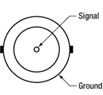
High Z Load: 10 V (Max); 50 Ω Load: 1.5 V (Max) for PDB220A2(/M), PDB210A(/M), PDB210C(/M), and PDB250x
High Z Load: 10 V; 50 Ω Load: 1.55 V (Max) for PDB230A and PDB230C
RF Output
BNC Female

High Z Load: 10 V (Max); 50 Ω Load: 3.5 V (Max) for PDB220A2(/M), PDB210A(/M), and PDB210C(/M)
High Z Load: 10 V (Max); 50 Ω Load: 2.5 V (Max) for PDB250x
High Z Load: ±4.0 V; 50 Ω Load: ±1.9 V for PDB230A and PDB230C
Power Connector Female (Photodetector)
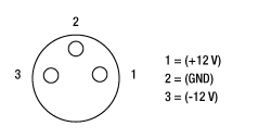
Power Connector Male (Power Cables)
OPERATION
Thorlabs' Free-Space Balanced Amplified Photodetectors consist of two well-matched photodiodes and an ultra-low noise, high-speed transimpedance amplifier (TIA) that generates an output voltage (RF OUTPUT) proportional to the difference between the photocurrents in the two photodiode (i.e., the two optical input signals). Additionally, the unit has two monitor outputs (MONITOR + and MONITOR -) to observe the optical input power levels on each photodiode.
SHIPPING LIST
PHOTODIODE TUTORIAL
Photodiode Tutorial
Theory of Operation
A junction photodiode is an intrinsic device that behaves similarly to an ordinary signal diode, but it generates a photocurrent when light is absorbed in the depleted region of the junction semiconductor. A photodiode is a fast, highly linear device that exhibits high quantum efficiency and may be used in a variety of different applications.
It is necessary to be able to correctly determine the level of the output current to expect and the responsivity based upon the incident light. Depicted in Figure 1 is a junction photodiode model with basic discrete components to help visualize the main characteristics and gain a better understanding of the operation of Thorlabs' photodiodes.

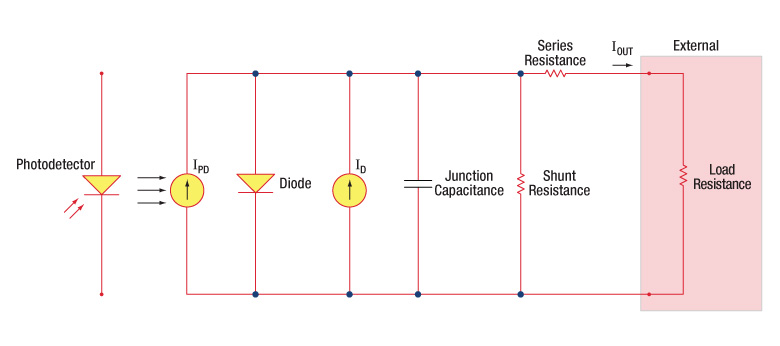
Figure 1: Photodiode Model
Photodiode Terminology
Responsivity
The responsivity of a photodiode can be defined as a ratio of generated photocurrent (IPD) to the incident light power (P) at a given wavelength:

Modes of Operation (Photoconductive vs. Photovoltaic)
A photodiode can be operated in one of two modes: photoconductive (reverse bias) or photovoltaic (zero-bias). Mode selection depends upon the application's speed requirements and the amount of tolerable dark current (leakage current).
Photoconductive
In photoconductive mode, an external reverse bias is applied, which is the basis for our DET series detectors. The current measured through the circuit indicates illumination of the device; the measured output current is linearly proportional to the input optical power. Applying a reverse bias increases the width of the depletion junction producing an increased responsivity with a decrease in junction capacitance and produces a very linear response. Operating under these conditions does tend to produce a larger dark current, but this can be limited based upon the photodiode material. (Note: Our DET detectors are reverse biased and cannot be operated under a forward bias.)
Photovoltaic
In photovoltaic mode the photodiode is zero biased. The flow of current out of the device is restricted and a voltage builds up. This mode of operation exploits the photovoltaic effect, which is the basis for solar cells. The amount of dark current is kept at a minimum when operating in photovoltaic mode.
Dark Current
Dark current is leakage current that flows when a bias voltage is applied to a photodiode. When operating in a photoconductive mode, there tends to be a higher dark current that varies directly with temperature. Dark current approximately doubles for every 10 °C increase in temperature, and shunt resistance tends to double for every 6 °C rise. Of course, applying a higher bias will decrease the junction capacitance but will increase the amount of dark current present.
The dark current present is also affected by the photodiode material and the size of the active area. Silicon devices generally produce low dark current compared to germanium devices which have high dark currents. The table below lists several photodiode materials and their relative dark currents, speeds, spectral ranges, and costs.
| Material | Dark Current | Speed | Spectral Range | Cost |
|---|---|---|---|---|
| Silicon (Si) | Low | High Speed | Visible to NIR | Low |
| Black Silicon (B-Si) | Low | Medium Speeda | Visible to NIR | Moderate |
| Germanium (Ge) | High | Low Speed | NIR | Low |
| Indium Gallium Arsenide (InGaAs) | Low | High Speed | NIR | Moderate |
| Indium Arsenide Antimonide (InAsSb) | High | Low Speed | NIR to MIR | High |
| Extended Range Indium Gallium Arsenide (InGaAs) | High | High Speed | NIR | High |
| Mercury Cadmium Telluride (MCT, HgCdTe) | High | Low Speed | NIR to MIR | High |
Junction Capacitance
Junction capacitance (Cj) is an important property of a photodiode as this can have a profound impact on the photodiode's bandwidth and response. It should be noted that larger diode areas encompass a greater junction volume with increased charge capacity. In a reverse bias application, the depletion width of the junction is increased, thus effectively reducing the junction capacitance and increasing the response speed.
Bandwidth and Response
A load resistor will react with the photodetector junction capacitance to limit the bandwidth. For best frequency response, a 50 Ω terminator should be used in conjunction with a 50 Ω coaxial cable. The bandwidth (fBW) and the rise time response (tr) can be approximated using the junction capacitance (Cj) and the load resistance (RLOAD):

Noise Equivalent Power
The noise equivalent power (NEP) is the input signal power that results in a signal-to-noise ratio (SNR) of 1 in a 1 Hz output bandwidth. This is useful, as the NEP determines the ability of the detector to detect low level light. In general, the NEP increases with the active area of the detector and is given by the following equation:

Here, S/N is the Signal to Noise Ratio, Δf is the Noise Bandwidth, and Incident Energy has units of W/cm2. For more information on NEP, please see Thorlabs' Noise Equivalent Power White Paper.
Terminating Resistance
A load resistance is used to convert the generated photocurrent into a voltage (VOUT) for viewing on an oscilloscope:

Depending on the type of the photodiode, load resistance can affect the response speed. For maximum bandwidth, we recommend using a 50 Ω coaxial cable with a 50 Ω terminating resistor at the opposite end of the cable. This will minimize ringing by matching the cable with its characteristic impedance. If bandwidth is not important, you may increase the amount of voltage for a given light level by increasing RLOAD. In an unmatched termination, the length of the coaxial cable can have a profound impact on the response, so it is recommended to keep the cable as short as possible.
Shunt Resistance
Shunt resistance represents the resistance of the zero-biased photodiode junction. An ideal photodiode will have an infinite shunt resistance, but actual values may range from the order of ten Ω to thousands of MΩ and is dependent on the photodiode material. For example, and InGaAs detector has a shunt resistance on the order of 10 MΩ while a Ge detector is in the kΩ range. This can significantly impact the noise current on the photodiode. For most applications, however, the high resistance produces little effect and can be ignored.
Series Resistance
Series resistance is the resistance of the semiconductor material, and this low resistance can generally be ignored. The series resistance arises from the contacts and the wire bonds of the photodiode and is used to mainly determine the linearity of the photodiode under zero bias conditions.
Common Operating Circuits
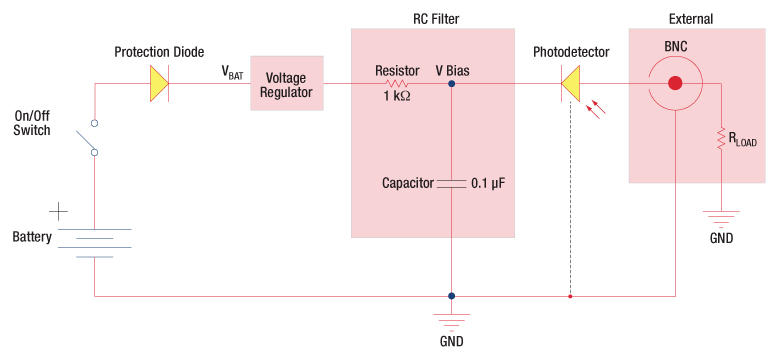
Figure 2: Reverse-Biased Circuit (DET Series Detectors)
The DET series detectors are modeled with the circuit depicted above. The detector is reverse biased to produce a linear response to the applied input light. The amount of photocurrent generated is based upon the incident light and wavelength and can be viewed on an oscilloscope by attaching a load resistance on the output. The function of the RC filter is to filter any high-frequency noise from the input supply that may contribute to a noisy output.
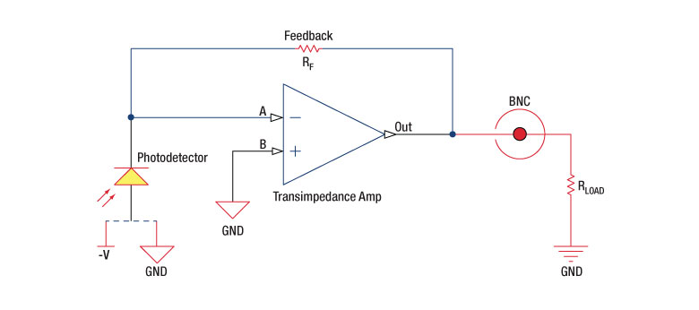
Figure 3: Amplified Detector Circuit
One can also use a photodetector with an amplifier for the purpose of achieving high gain. The user can choose whether to operate in Photovoltaic of Photoconductive modes. There are a few benefits of choosing this active circuit:
- Photovoltaic mode: The circuit is held at zero volts across the photodiode, since point A is held at the same potential as point B by the operational amplifier. This eliminates the possibility of dark current.
- Photoconductive mode: The photodiode is reversed biased, thus improving the bandwidth while lowering the junction capacitance. The gain of the detector is dependent on the feedback element (Rf). The bandwidth of the detector can be calculated using the following:
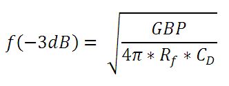
where GBP is the amplifier gain bandwidth product and CD is the sum of the junction capacitance and amplifier capacitance.
Effects of Chopping Frequency
The photoconductor signal will remain constant up to the time constant response limit. Many detectors, including PbS, PbSe, HgCdTe (MCT), and InAsSb, have a typical 1/f noise spectrum (i.e., the noise decreases as chopping frequency increases), which has a profound impact on the time constant at lower frequencies.
The detector will exhibit lower responsivity at lower chopping frequencies. Frequency response and detectivity are maximized for
![]()
Free-Space Balanced Amplified Photodetectors, DC - 1 MHz, Fixed Gain
Part Number | Description | Price | Availability |
|---|---|---|---|
PDB220A2/M | Free-Space Balanced Photodetector, UV-Enhanced Si, 4.1 mm Active Diameter, 190-1100 nm, M4 Taps | $1,264.28 | Today |
PDB210A/M | Free-Space Balanced Photodetector, Si, 5 mm Active Diameter, 320-1060 nm, M4 Taps | $1,171.92 | Today |
PDB210C/M | Free-Space Balanced Photodetector, InGaAs, 3 mm Active Diameter, 800-1700 nm, M4 Taps | $2,184.31 | Lead Time |
PDB220A2 | Free-Space Balanced Photodetector, UV-Enhanced Si, 4.1 mm Active Diameter, 190-1100 nm, 8-32 Taps | $1,264.28 | Lead Time |
PDB210A | Free-Space Balanced Photodetector, Si, 5 mm Active Diameter, 320-1060 nm, 8-32 Taps | $1,171.92 | Today |
PDB210C | Free-Space Balanced Photodetector, InGaAs, 3 mm Active Diameter, 800-1700 nm, 8-32 Taps | $2,184.31 | Today |
Free-Space Balanced Amplified Photodetectors, DC - 100 MHz, Fixed Gain
Part Number | Description | Price | Availability |
|---|---|---|---|
PDB230A | Customer Inspired! Free-Space Balanced Photodetector, Si, 0.8 mm Active Diameter, 320-1000 nm, 8-32 and M4 Combi Thread | $1,385.61 | Today |
PDB230C | Customer Inspired! Free-Space Balanced Photodetector, InGaAs, 0.3 mm Active Diameter, 800-1700 nm, 8-32 and M4 Combi Thread | $1,995.27 | Today |
Free-Space Balanced Amplified Photodetectors, DC - 1 MHz, Switchable Gain
Click to Enlarge
PDB250x Series Power Switch and Gain Selector
Part Number | Description | Price | Availability |
|---|---|---|---|
PDB250A2 | Customer Inspired! Switchable Gain Free-Space Balanced Photodetector, UV-Enhanced Si, 4.1 mm Active Diameter, 190-1100 nm, 8-32 / M4 Combi Thread | $1,366.80 | Today |
PDB250A | Customer Inspired! Switchable Gain Free-Space Balanced Photodetector, Si, 5 mm Active Diameter, 320-1060 nm, 8-32 / M4 Combi Thread | $1,275.00 | Today |
PDB250C | Customer Inspired! Switchable Gain Free-Space Balanced Photodetector, InGaAs, 3 mm Active Diameter, 800-1700 nm, 8-32 / M4 Combi Thread | $2,284.80 | Today |
±12 VDC Regulated Linear Power Supply
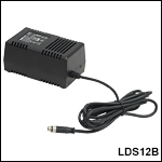
- Replacement Power Supply for the Balanced Amplified Photodetectors Sold Above
- ±12 VDC Power Output
- Current Limit Enabling Short Circuit and Overload Protection
- On/Off Switch with LED Indicator
- Switchable AC Input Voltage (100, 120, or 230 VAC)
- 2 m (6.6') Cable with LUMBERG RSMV3 Male Connector
- UL and CE Compliant
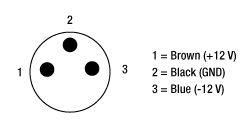
The LDS12B ±12 VDC Regulated Linear Power Supply is intended as a replacement for the supply included with our PDB line of balanced photodetectors sold on this page. The cord has three pins: one for ground, one for +12 V, and one for -12 V (see diagram to the right). A region-specific power cord is shipped with the unit based on your location. This power supply can also be used with the PDA series of amplified photodetectors, PMM series of photomultiplier modules, APD series of avalanche photodetectors, and the FSAC autocorrelator for femtosecond lasers.
Part Number | Description | Price | Availability |
|---|---|---|---|
LDS12B | ±12 VDC Regulated Linear Power Supply, 6 W, 100/120/230 VAC | $93.55 | Today |

