Lithium Niobate Electro-Optic Modulators, Fiber-Coupled (1260 nm - 1625 nm)
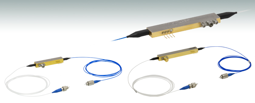
- Up to 40 GHz Lithium Niobate (LiNbO3) Modulators
- Fiber-Coupled, High-Speed Modulation
- Intensity, Phase, or I/Q
- X-Cut or Z-Cut Devices
LNP6118
40 GHz Phase Modulator with Polarizer, Z-Cut
LNA2322
10 GHz Intensity Modulator,
X-Cut
LNLVL-IM-Z
Low Vπ 40 GHz Intensity Modulator, Z-Cut
Enlarged View
OVERVIEW

Click to Enlarge
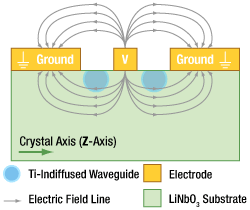
Z-Cut LiNbO3 Intensity Modulator Cross-Section
Click to Enlarge
X-Cut LiNbO3 Intensity Modulator Cross-Section
Features
- Titanium-Indiffused Waveguides
- Low Optical Loss
- Long-Term Bias Stability
- Hermetically Sealed Packaging
- FC/PC Fiber Connectors
Thorlabs manufactures a variety of lithium niobate (LiNbO3) optical phase, intensity, and I/Q modulators. These high-performance devices are based on titanium-indiffused waveguide technology, offer large bandwidths, and are ideal for developing high-speed modulation systems.
The modulators on this page are fabricated from either X-cut or Z-cut LiNbO3 (see the example diagrams to the right). X-cut intensity modulators employ a symmetrical design that provides low frequency-chirp in the modulated signal, while Z-cut intensity modulators provide more efficient modulation (i.e., lower Vπ or half-wave voltage) at the expense of higher frequency-chirp. Phase modulators are only offered as Z-cut devices because their single optical path does not benefit from the symmetry of the X-cut design. The I/Q modulator fully exploits the advantages of symmetry as an X-cut device.
Z-cut devices are also capable of supporting both the ordinary and extraordinary optical modes, which have different modulation efficiencies. An integrated optical polarizer, positioned before the output port of the device, is included in all of our Z-cut intensity modulators and some of our Z-cut phase modulators as only one mode is desirable for most applications. While most applications benefit from the integrated polarizer, the LN53S-FC, LNP6119, and LNP4217 Z-cut phase modulators are offered for applications where the polarizer is undesirable.
The modulators come with a polarization-maintaining (PM) input fiber pigtail and a single-mode (SM) output fiber pigtail that are terminated with FC/PC connectors. The PM fiber is keyed to the slow axis, which is also aligned to the extraordinary mode of the modulator. Please note that custom options for PM output fiber pigtails and FC/APC connectors are available for all LiNbO3 modulators. For more information on custom configurations (e.g., fiber type, connectors) and quotes, please contact Tech Support.
All the fiber-coupled LiNbO3 modulators offered below are compatible with our EO modulator drivers. Our fiber-coupled tunable lasers provide an ideal O-band, C-band, or L-band source for use with these modulators. For all-in-one solutions in high-speed fiber optic test and measurement, we offer reference transmitters, optical transmitter with phase modulators, and calibrated electrical-to-optical converters.
SPECS
| Maximum Ratings for LiNbO3 Modulators | |
|---|---|
| Optical Input Power | 100 mW |
| Input RF Power | 24 dBm |
| Operating Temperature Range | 0 °C to 70 °C |
| Storage Temperature Range | -40 °C to 85 °C |
Intensity Modulator Specifications
| Item # | LNA2322 | LNA2124 | LNA6213 | LNA6112 | LNLVL-IM-Z |
|---|---|---|---|---|---|
| Optical | |||||
| Operating Wavelengtha | 1525 nm - 1605 nm | 1525 nm - 1605 nm | 1260 nm - 1625 nm | 1525 nm - 1605 nm | 1525 nm - 1605 nm |
| Optical Insertion Loss | ≤5.0 dB (4.0 dB Typ.) | ≤5.0 dB (4.0 dB Typ.) | ≤6.5 dB (5.0 dB Typ.) @ 1310 nm ≤5.5 dB (4.5 dB Typ.) @ 1550 nm |
≤5.0 dB (4.0 dB Typ.) | ≤5.5 dB (4.5 dB Typ.) |
| Optical Return Loss | ≥40 dB | ≥40 dB | ≥40 dB | ≥40 dB | ≥40 dB |
| Optical Extinction Ratio (@ DC, 1550 nm) |
≥20 dB | ≥20 dB | ≥20 dB | ≥20 dB | ≥20 dB |
| Optical Input Power (Extraordinary Mode) | ≤100 mW | ||||
| Optical Input Power (Ordinary Mode) |
≤100 mW | ≤10 mWb | |||
| Electrical (@ 1550 nm) | |||||
| E/O Bandwidth (-3 dB) | ≥10 GHz (14 GHz Typ.) | ≥10 GHz (15 GHz Typ.) | ≥30 GHz (35 GHz Typ.) | ≥30 GHz (35 GHz Typ.) | 10 GHz (Typ.) |
| Operating Frequency Range | DC to 15 GHz (Min) | DC to 15 GHz (Min) | DC to 40 GHz (Min) | DC to 40 GHz (Min) | DC to 40 GHz (Min) |
| RF Vπ (@ 1 GHz) | ≤6.5 V (4.5 V Typ.) | ≤6.5 V (4.3 V Typ.) | ≤6.0 V (5.5 V Typ.) | ≤6.0 V (5.5 V Typ.) | 2.2 V (Typ.) |
| RF Vπ (@ 20 GHz) | - | - | - | - | ≤3.9 V (3.5 V Typ.) |
| RF Vπ (@ 40 GHz) | - | - | - | - | ≤6.0 V (5.0 V Typ.) |
| DC Bias Vπ (@ 1 kHz) | ≤10.0 V (6.5 V Typ.) | ≤15.0 V (13.0 V Typ.) | ≤5.0 V (3.5 V Typ.) | ≤11.0 V (8.5 V Typ.) | ≤11.0 V (9.0 V Typ.) |
| S11 | -12 dB (-10 dB Max), DC to 10 GHz | -12 dB (-10 dB Max), DC to 25 GHz -8 dB (-6 dB Max), 25 to 40 GHz |
|||
| RF Input Power | 24 dBm Maximum | ||||
| Photodetector | |||||
| Reverse Bias Voltage | -5.5 V to -3.0 V | N/A | |||
| Responsivity | 0.1 mA/mW to 0.5 mA/mW | N/A | |||
| Output Optical Power Monitoring Range |
-5 dBm to 10 dBm | N/A | |||
| Mechanical | |||||
| Crystal Orientation | X-Cut | Z-Cut | Z-Cut | Z-Cut | Z-Cut |
| RF Connection | Male SMP (GPO®† Compatible), Full Detent | Female 1.85 mm (V) | Female 1.85 mm (V) | Female 2.92 mm (K) | |
| Fiber Type | Input: PANDA Polarization Maintaining Output: SMF-28®† Single Mode |
||||
| Fiber Lead Length | 1.5 m Typ. | ||||
| Internal Polarizer | N/Ac | Aligned with the Extraordinary Mode of the Chip | Aligned with the Extraordinary Mode of the Chip | Aligned with the Extraordinary Mode of the Chip | Aligned with the Extraordinary Mode of the Chip |
| Environmental | |||||
| Operating Case Temperature | 0 °C to 70 °C | ||||
| Storage Temperature | -40 °C to 85 °C | ||||
Phase Modulator Specifications
| Item # | LN65S-FC | LN53S-FC | LNP6118 | LNP6119 | LNP4216 | LNP4217 |
|---|---|---|---|---|---|---|
| Optical | ||||||
| Operating Wavelengtha | 1525 nm - 1605 nm | 1260 nm - 1625 nm | 1260 nm - 1625 nm | |||
| Optical Insertion Loss | ≤4.5 dB (3.0 dB Typ.) | ≤5.5 dB (5.0 dB Typ.) @ 1310 nm ≤4.5 dB (4.0 dB Typ.) @ 1550 nm |
≤7.25 dB (6.0 dB Typ.) @ 1310 nm ≤5.75 dB (5.0 dB Typ.) @ 1550 nm |
|||
| Optical Return Loss | ≥40 dB | |||||
| Optical Input Power (Extraordinary Mode) |
≤100 mW | |||||
| Optical Input Power (Ordinary Mode) |
≤10 mWb | ≤100 mW | ≤10 mWb | ≤100 mW | ≤10 mWb | ≤100 mW |
| Electrical (@ 1550 nm) | ||||||
| S11 | -12 dB (-10 dB Max), DC to 10 GHz | -12 dB (-10 dB Max), DC to 25 GHz -8 dB (-6 dB Max), 25 to 40 GHz |
||||
| E/O Bandwidth (-3 dB) | 10 GHz Typ. | 35 GHz Typ. | 10 GHz Typ. | |||
| Operating Frequency Range | DC to 15 GHz (Min) | DC to 40 GHz (Min) | DC to 40 GHz (Min) | |||
| RF Vπ (@ 10 GHz) | 6.5 V (Typ.) | 7.0 V (Typ.) | 3.5 V (Typ.) | |||
| RF Vπ (@ 30 GHz) | - | ≤9.5 V (8.5 V Typ.) | ≤5.5 V (4.6 V Typ.) | |||
| RF Input Power | 24 dBm Maximum | |||||
| Low-Frequency Modulator Specifications (@ 1550 nm) | ||||||
| Operating Frequency Range | N/A | DC to 1 MHz (Typ.) | DC to 1 MHz (Typ.) | |||
| Vπ | N/A | 10 V (Typ.) @ 1 kHz | 13 V (Typ.) @ 1 kHz | |||
| Mechanical | ||||||
| Crystal Orientation | Z-Cut | |||||
| RF Connection | Male SMP (GPO®† Compatible), Full Detent | Female 1.85 mm (V) | Female 2.92 mm (K) | |||
| Fiber Type | Input: PANDA Polarization Maintaining Output: SMF-28®† Single Mode |
|||||
| Fiber Lead Length | 1.5 m Typ. | |||||
| Internal Polarizer | Aligned with the Extraordinary Mode of the Chip | N/Ac | Aligned with the Extraordinary Mode of the Chip | N/Ac | Aligned with the Extraordinary Mode of the Chip | N/Ac |
| Environmental | ||||||
| Operating Case Temperature | 0 °C to 70 °C | |||||
| Storage Temperature | -40 °C to 85 °C | |||||
I/Q Modulator Specifications
| Item # | LNQ4314 |
|---|---|
| Optical | |
| Operating Wavelengtha | 1525 nm - 1575 nm |
| Optical Insertion Loss | ≤9.0 dB (7.0 dB Typ.) |
| Optical Return Loss | ≥40 dB |
| Optical Extinction Ratio | ≥20 dB |
| Optical Input Power | ≤100 mW |
| Electrical | |
| S11 | -12 dB (-10 dB Max), DC to 25 GHz -8 dB (-6 dB Max), 25 to 30 GHz |
| E/O Bandwidth (-3 dB) | ≥20 GHz (25 GHz Typ.) |
| Operating Frequency Range | DC to 30 GHz |
| RF Vπ (@ 1 GHz) | ≤7.5 V (6.0 V Typ.) |
| DC Biases Vπ (@ 1 kHz) | ≤10.0 V (8.0 V Typ.) |
| RF Input Power | 24 dBm Maximum |
| Mechanical | |
| Crystal Orientation | X-Cut |
| RF Connections (Two) | Male SMPM (GPPO®† Compatible), Full Detent |
| Fiber Type | Input: PANDA Polarization Maintaining Output: SMF-28®† Single Mode |
| Fiber Lead Length | 1.5 m Typ. |
| Environmental | |
| Operating Case Temperature | 0 °C to 70 °C |
| Storage Temperature | -40 °C to 85 °C |
† GPO, GPPO, and SMF-28 are registered trademarks of Corning Incorporated.
PIN DIAGRAMS
Intensity Modulator Pin Diagrams

Click to Enlarge
LNA2322 10 GHz Intensity Modulator, X-Cut, Pin Diagram

Click to Enlarge
LNA2124 10 GHz Intensity Modulator, Z-Cut, Pin Diagram
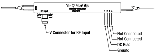
Click to Enlarge
LNA6213 40 GHz Intensity Modulator Pin Diagram
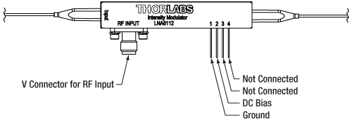
Click to Enlarge
LNA6112 Small Form Factor Housing 40 GHz Intensity Modulator Pin Diagram

Click to Enlarge
LNLVL-IM-Z Low Vπ 40 GHz Intensity Modulator Pin Diagram
Phase Modulator Pin Diagrams
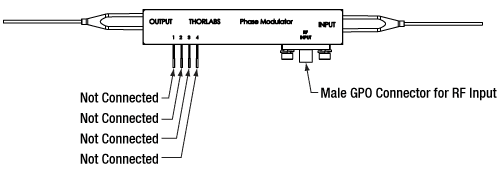
Click to Enlarge
LN65S-FC and LN53S-FC 10 GHz Phase Modulator Pin Diagram
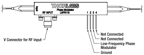
Click to Enlarge
LNP6118 and LNP6119 40 GHz Phase Modulator Pin Diagram

Click to Enlarge
LNP4216 and LNP4217 Low Vπ 40 GHz Phase Modulator Pin Diagram
I/Q Modulator Pin Diagram
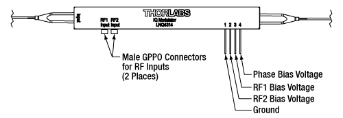
Click to Enlarge
LNQ4314 25 GHz I/Q Modulator Pin Diagram
LAB FACTS
Driving an Electro-Optic Phase Modulator with the Amplified Output of a Function Generator
Click to Enlarge
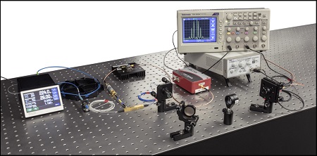
Figure 1: Experimental Setup Used to Evaluate Whether a Basic RF Source Built Around a Function Generator Could be Sufficient to Drive a Fiber-Coupled EO Phase Modulator
Thorlabs offers a selection of fiber-coupled electro-optic (EO) modulators, which are ideal for modulating light from fiber-coupled laser sources. Applications frequently require EO modulators to be driven at rates of 1 GHz or higher, which places significant demands on the driving radio frequency (RF) voltage source. We investigated whether it would be possible to use a basic setup built around a function generator to drive a fiber-coupled EO phase modulator. The experimental setup we designed and implemented to test this possibility included instrumentation to record the spectrum of the modulated optical signal. By analyzing the modulated optical spectrum, we confirmed this basic RF source is a viable option for driving a fiber-coupled EO phase modulator. Our approach and results are documented in this Lab Fact.
Experimental Design and Setup
The design of the RF voltage source portion of the setup required first determining the power the RF source should supply to drive the fiber-coupled EO phase modulator. The power requirements were calculated after we made an estimate of the driving voltage needed to achieve the modulation depth desired for this application. Details describing our process for selecting a modulation depth, the relationship between modulation depth and driving voltage, and the calculations we used to estimate the power required from the RF voltage source are included in the Lab Facts document. From our investigations, we determined the power from the function generator alone would not be sufficient for our application. Our solution was to insert a low noise amplifier between the function generator and EO modulator. We also included an electrical low pass filter before the modulator to remove signal distortion that appeared to originate with the function generator. We drove the EO phase modulator with a sinusoidal RF voltage, which imparted a sinusoidal phase modulation on the 1550 nm CW laser signal.
A scanning Fabry-Perot interferometer, whose output was sent to an oscilloscope, was placed after the EO phase modulator and used to measure and monitor the spectrum of the modulated optical signal. It was necessary to use the Fabry-Perot interferometer for this purpose as it has the ability to resolve the very fine spectral features of the phase-modulated optical spectra: at a wavelength of 1550 nm, a frequency difference of 1 GHz is equivalent to a wavelength difference of 0.8 pm. The measured spectra were recorded as functions of scan time. In the Lab Facts document, we describe a straight-forward method to convert from units of Fabry-Perot scan time to units of relative optical frequency. For this work, we estimate Δf = (1.17 GHz/ms)Δt.
Experimental Results
As is described in the Lab Facts document, theory predicts the spectra of our phase modulated optical signals would include sets of symmetric sidebands arranged around the laser carrier peak at frequency fo. The sidebands are displaced from the laser carrier peak frequency at integer multiples of the modulation frequency fm (fo ± Nfm with N = 1, 2, ...). The relative heights of the sidebands are a function of the modulation depth, which is in turn a function of the peak-to-peak value of the RF driving voltage. Given the modulation depth, the relative amplitudes of the laser carrier peak and modulation sidebands can be calculated. This makes it possible to tailor the power distribution across the various peaks to meet an application's needs. We used the predictive power of this model to confirm our RF source was adequately driving the EO modulator.
The spectra shown in Figures 2 and 4 are representative of the modulation spectra we measured. The theoretical curves in Figure 3 are a function of modulation depth and plot the expected relative powers of the laser carrier peak (solid red curve), first order sidebands (dotted blue curve), second order sidebands (dotted green curve), and third order sidebands (dotted violet curve). The black arrow points to the modulation depth corresponding to the spectrum in Figure 2, and the gray arrow points to the modulation depth corresponding to the spectrum in Figure 4. From our results, we determined our measured and applied modulation frequencies agreed, and we confirmed the spectral power distributions in our optical spectra were consistent with the peak-to-peak driving voltage of the RF source. We conclude that the good agreement between the expected and recorded results validates the use of a basic RF source built around a function generator as a driver for fiber-coupled EO phase modulators.

Click to Enlarge
Figure 4: EO Phase Modulator Spectrum When Vpp = 3.63 V
The carrier frequency is fo; the modulation frequency is fm = 1 GHz. The X-axis reports the scanning time of the Fabry-Perot interferometer and can be directly related to the signal's relative frequency spectrum.

Click to Enlarge
Figure 3: Curves Relating the Power in the Carrier and Several Sideband Peaks as A Function of Modulatrion Depth
The 0.44 modulation depth indicated by the black arrow corresponds to Figure 2, and the 0.56 modulation depth indicated by the gray arrow corresponds to Figure 4.

Click to Enlarge
Figure 2: EO Phase Modulator Spectrum When Vpp = 2.85 V
The carrier frequency is fo; the modulation frequency is fm = 1 GHz. The X-axis reports the scanning time of the Fabry-Perot interferometer and can be directly related to the signal's relative frequency spectrum.
Intensity Modulators


Click to Enlarge
This operational diagram of an intensity modulator shows the waveguide (blue lines) splitting into two paths embedded in the surface of the lithium niobate (green). The input light is first affected by the modulating RF drive voltage and then the DC bias voltage, as shown by the translucent regions.
Applications
- RF-Over-Fiber (RFOF) and Microwave Photonics
- High-Speed Telecommunications
- WDM Transmission
LiNbO3 optical intensity modulators use a Mach-Zehnder interferometer structure to allow modulation of the optical output power of the device, as shown by the operational diagram to the right. The devices include two electrical ports: one for the modulation driving signal and one for biasing the modulator. X-cut or Z-cut devices are available. Each modulator has field-replaceable RF input connectors.
X-cut devices allow for both arms of the Mach-Zehnder interferometer to be symmetrically modulated. This symmetry ensures that the modulated output is not also shifted in phase/frequency (chirped).
Z-cut devices have an inequality in the push-pull phase shift between the two arms of the Mach-Zehnder interferometer. This results in a phase/frequency shift (chirp) in the output in addition to the intensity modulation. Z-cut devices also have a better overlap of the electrical and optical fields in the Mach-Zehnder structure, resulting in higher drive efficiencies.
The LNA2322 10 GHz modulator includes an integrated photodetector for optical power monitoring and modulator bias control, eliminating the need for an external fiber tap.
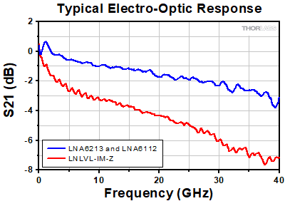
Thorlabs offers three high-speed intensity modulators that can operate up to 40 GHz. The LNA6213 modulator is a high bandwidth device designed to provide up to 40 GHz of modulation over the 1260 nm to 1625 nm operating range. The LNA6112 modulator provides similar performance as the LNA6213, but in the 1525 nm to 1605 nm wavelength range and has a small form factor housing that is 105.0 mm wide compared to the 135.0 mm housings of the other high-speed intensity modulators. The LNLVL-IM-Z modulator provides the lowest RF Vπ, or half-wave voltage, at any specific frequency over the operating frequency range. The graphs below show a typical drive voltage (left) and electro-optic response (right) over the operating frequency range for these modulators. See the Specs tab for complete specifications.
Part Number | Description | Price | Availability |
|---|---|---|---|
LNA2322 | 10 GHz Intensity Modulator with Internal Photodetector, X-Cut, FC/PC Connectors, 1525 nm - 1605 nm | $3,549.00 | Today |
LNA2124 | 10 GHz Intensity Modulator, Z-Cut, FC/PC Connectors, 1525 nm - 1605 nm | $3,549.00 | Today |
LNA6213 | 40 GHz Intensity Modulator, Z-Cut, FC/PC Connectors, 1260 nm - 1625 nm | $5,903.96 | Lead Time |
LNA6112 | Customer Inspired! 40 GHz Intensity Modulator, Z-Cut, FC/PC Connectors, 1525 nm - 1605 nm, Small Form Factor Housing | $4,964.09 | Today |
LNLVL-IM-Z | Low Vπ Intensity Modulator, Z-Cut, FC/PC Connectors, Operational up to 40 GHz, 1525 nm - 1605 nm | $5,903.96 | Today |
Phase Modulators


Click to Enlarge
This operational diagram of a phase modulator shows the waveguide (blue line) as one through optical path embedded in the surface of the lithium niobate (green). The input light is affected only by the modulating RF drive voltage, as shown by the translucent region.
Applications
- Chirp Control for High-Speed Communications
- Coherent Communications
- Optical Sensing
LiNbO3 optical phase modulators consist of a single, through optical waveguide, as shown by the operational diagram to the right. As there is only one optical path to modulate, all of the phase modulators are Z-cut devices in order to optimize drive efficiency. Each modulator has field-replaceable RF input connectors.
The LN65S-FC and LN53S-FC phase modulators provide up to 10 GHz of modulation over the 1525 nm to 1605 nm operating range. The LNP6118 and LNP6119 modulators are high bandwidth devices that provide up to 40 GHz of modulation over the 1260 nm to 1625 nm range.
The LNP4216 and LNP4217 phase modulators provide lower RF Vπ, or half-wave voltage, over the operating frequency range compared to the LNP6118 and LNP6119 modulators. The typical drive voltage of the LNP421x modulators is 3.5 V at 10 GHz and 4.6 V at 30 GHz, compared to the LNP611x modulators that have typical drive voltage of 7.0 V at 10 GHz and 8.5 V at 30 GHz. These devices can be operated at frequencies up to 40 GHz over the 1260 nm to 1625 nm range.
The LNP6118, LNP6119, LNP4216, and LNP4217 devices incorporate an additional low-frequency phase modulator, in series with the RF phase modulator, that can be controlled through a separate set of pins (see the Specs and Pin Diagrams tabs for details).
When only one mode is desired, the LN65S-FC, LNP6118, and LNP4216 modulators include an internal polarizer that is aligned with the extraordinary mode of the chip. For applications that require access to both the ordinary and extraordinary modes, the LN53S-FC, LNP6119, and LNP4217 Z-cut phase modulators are offered without an integrated polarizer.
Part Number | Description | Price | Availability |
|---|---|---|---|
LN65S-FC | 10 GHz Phase Modulator, FC/PC Connectors, 1525 nm - 1605 nm | $3,169.00 | Today |
LN53S-FC | 10 GHz Phase Modulator without Polarizer, FC/PC Connectors, 1525 nm - 1605 nm | $3,169.00 | Today |
LNP6118 | 40 GHz Phase Modulator, FC/PC Connectors, 1260 nm - 1625 nm, Small Form Factor Housing | $4,964.09 | Today |
LNP6119 | 40 GHz Phase Modulator without Polarizer, FC/PC Connectors, 1260 nm - 1625 nm, Small Form Factor Housing | $4,964.09 | Today |
LNP4216 | Low Vπ Phase Modulator, FC/PC Connectors, Operational up to 40 GHz, 1260 nm - 1625 nm | $5,903.96 | Lead Time |
LNP4217 | Low Vπ Phase Modulator without Polarizer, FC/PC Connectors, Operational up to 40 GHz, 1260 nm - 1625 nm | $5,903.96 | Today |
I/Q Modulator


Click to Enlarge
This operational diagram of an I/Q modulator shows the waveguides (blue lines) split into four paths embedded in the surface of the lithium niobate (green). The input light is first affected by each MZI's modulating RF drive voltage (RF1 or RF2), and then by each MZI's DC bias voltage (DC1 or DC2), as shown by the translucent regions.
- Dual, Parallel MZIs on a Single X-Cut Lithium Niobate Chip
Applications
- Coherent Communications, Including QAM, QPSK, and DQPSK Encoding
- Single Side Band Suppressed Carrier (SSB-SC) Transmission
LiNbO3 I/Q modulators use a dual-parallel Mach-Zehnder interferometer (MZI) structure in order to allow modulation of both the phase and amplitude of light for advanced optical transmission schemes. As shown in the operational diagram to the right, the modulator consists of two independently-controlled MZIs whose outputs are combined. The combining structure also includes a bias electrode that applies a phase delay between the two MZIs, allowing for the required phase control between the two modulator arms.
In a QPSK application, this device will allow for a 50 Gb/s link transmission rate. Two I/Q modulators can be used together in a polarization-multiplexed arrangement to double the transmission rate, e.g. two LNQ4314 devices can provide a 100 Gb/s link on the same optical channel/wavelength.
Part Number | Description | Price | Availability |
|---|---|---|---|
LNQ4314 | 25 GHz I/Q Modulator, FC/PC Connectors, 1525 nm - 1575 nm | $7,122.90 | Today |


